Engineers Garage

  • Electronic Projects & Tutorials
    • Electronic Projects
      • Arduino Projects
      • AVR
      • Raspberry pi
      • ESP8266
      • BeagleBone
      • 8051 Microcontroller
      • ARM
      • PIC Microcontroller
      • STM32
    • Tutorials
      • Audio Electronics
      • Battery Management
      • Brainwave
      • Electric Vehicles
      • EMI/EMC/RFI
      • Hardware Filters
      • IoT tutorials
      • Power Tutorials
      • Python
      • Sensors
      • USB
      • VHDL
    • Circuit Design
    • Project Videos
    • Components
  • Articles
    • Tech Articles
    • Insight
    • Invention Stories
    • How to
    • What Is
  • News
    • Electronic Product News
    • Business News
    • Company/Start-up News
    • DIY Reviews
    • Guest Post
  • Forums
    • EDABoard.com
    • Electro-Tech-Online
    • EG Forum Archive
  • DigiKey Store
    • Cables, Wires
    • Connectors, Interconnect
    • Discrete
    • Electromechanical
    • Embedded Computers
    • Enclosures, Hardware, Office
    • Integrated Circuits (ICs)
    • Isolators
    • LED/Optoelectronics
    • Passive
    • Power, Circuit Protection
    • Programmers
    • RF, Wireless
    • Semiconductors
    • Sensors, Transducers
    • Test Products
    • Tools
  • Learn
    • eBooks/Tech Tips
    • Design Guides
    • Learning Center
    • Tech Toolboxes
    • Webinars & Digital Events
  • Resources
    • Digital Issues
    • EE Training Days
    • LEAP Awards
    • Podcasts
    • Webinars / Digital Events
    • White Papers
    • Engineering Diversity & Inclusion
    • DesignFast
  • Guest Post Guidelines
  • Advertise
  • Subscribe

Designing Gate Driver Circuit and Switching Mechanism for Modified Sine Wave Inverter – (Part 9/17)

By Dikhsa May 12, 2024

In the previous tutorial, basic operation of a modified sine wave inverter was discussed. It was mentioned in the previous tutorial that the H-bridge MOSFET circuit of the quasi sine wave inverter cannot be directly interfaced with the microcontroller circuit. There is a need of a Gate driver circuit as an intermediate circuit between the microcontroller and the H-bridge MOSFET circuit. The H-bridge MOSFET circuit generates a modified sine wave by switching the MOSFETs in a sequential manner with predetermined delay.
This sequential switching of the MOSFETs in the previous tutorial was explained with the help of a truth table and circuit diagrams. In this tutorial, designing and working of the intermediate gate driver circuitry will be discussed. After adding the gate driver circuitry, the resultant circuit will be able to generate a modified sine wave having a peak to peak voltage of 12 V. In the next tutorial, then, the inverter circuit will be completed by adding a switching mechanism and step up transformer. The output of that circuit will be a quasi sine wave having peak voltage of 220 V and frequency of 50 Hz.  
Why need gate driver circuit – 
In half bridge configuration, there are two MOSFETs where one of them is in low-side configuration and other is in high-side configuration. For driving the high side MOSFET the microcontroller cannot be directly interfaced to its gate terminal. There must be a gate driver circuit for switching the high side MOSFETs contrary to the low-side MOSFETs which can be directly operated without need of any external circuitry.
In order to learn more about low side configuration and high side configuration of MOSFET and the requirement of gate driver circuit for driving high side MOSFET, refer to the following tutorial – 
High and low side switching of MOSFET
Method for driving  full bridge or half bridge – 
The full bridge configuration is the combination of two half bridge circuits. So, it is first important to understand the half bridge circuit and its driving method. As high side MOSFET cannot be normally operated like low side MOSFETs, there are two methods of driving the high side MOSFET – one is through “dual power supply” and another is by using “bootstrap circuit”. In circuit designed here, bootstrap method is used to drive to the high side MOSFET. But the MOSFET cannot be driven with only bootstrap circuit. Their needs some extra circuit as well. That extra circuit can be incorporated by using some IC having the circuit inbuilt or by designing the circuit explicitly. In the circuit designed here, IR-2110 IC is used. This IC is cheap and easily available. Plus it can be easily used in any circuit. This IC can drive a half bridge circuit one at a time. So for full bridge configuration, there needs two IR2110 ICs. 

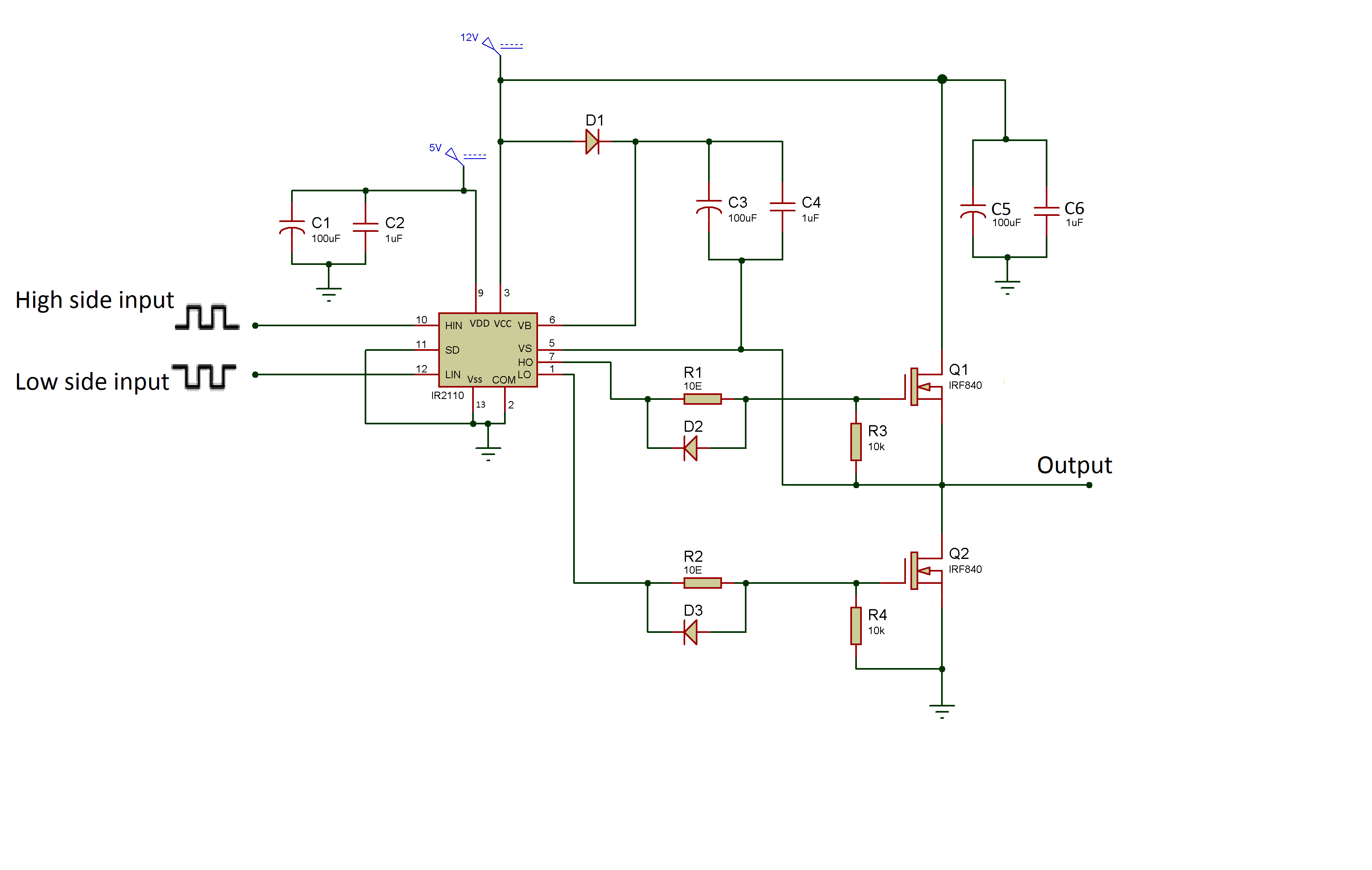
This IC drives the high side MOSFET using the external bootstrap circuit as well as the low side MOSFET (which do not require any external circuit). So, this IC suits best as per the requirement of the circuit.

Components Required – 
List of Components required for Gate Driver Circuit and Switching Mechanism for Modified Sine Wave Inverter
Fig. 1: List of components required for Gate Driver Circuit and Switching Mechanism for Modified Sine Wave Inverter
Block Diagram – 

Block Diagram of Modified Sine Wave Inverter

Fig. 2: Block Diagram of Modified Sine Wave Inverter 

Circuit Connections – 
In the previous tutorial, the control circuitry using the Arduino UNO was already designed. Now it’s time to design the switching mechanism and gate driver circuitry. The gate driver circuitry can be designed using IR-2110 IC. IR2110 is a high and low side driver IC. It is a high speed (operational at high frequency) power MOSFET and IGBT driver with independent high and low side referenced output channels. The floating channels can operate up to 500 V or 600 V. The IC is 3.3V logic compatible that is why it can be used with any microcontroller.
The IC comes in a 14 Lead PDIP package. IR2110 has the following pin configuration –
Table Listing Pin Configuration of IR-2110 IC
Fig. 3: Table listing pin configuration of IR-2110 IC
The IR-2110 has the following pin diagram – 
Pin Diagram of IR-2110 IC
Fig. 4: Pin Diagram of IR-2110 IC

Representational Image of IR-2110 IC

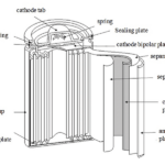
Fig. 5: Representational Image of IR-2110 IC

Lead/Pin assignments with pictorial representation of IR2110

The VCC is the low side voltage and should be in range from 10 V to 20 V. The VDD is the logic voltage for working of the internal circuitry of the IC. The VDD should range in between 3 V to 20 V (with reference to Vss). The actual voltage of VDD is decided by the input supply of Lin and Hin pin. The Lin and Hin pins are the input logic supply pins for driving the low or high side driver. When the input at Lin is high then this drives the low side driver and output at LO is equal to VCC. If the Lin pin is low this turns OFF the low side driver and output at LO is equal to COM (ground). Similarly, when the input at Hin is high then this drives the high side driver and output at HO is equal to VB. If the Hin pin is low this turns OFF the high side driver and output at HO is equal to Vs. This IC works on TTL or CMOS logic so for input greater than 3V it will give logic 1.  As the microcontroller is used for giving input signals to Lin and Hin pins and the controller works on TTL logic, VDD equal to 5V is used to avoid any undermine state at the output due to mismatching in VDD and logic input power supply. The Vss is the logic ground and COM is the low side return. Both are not internally connected to each other so they have been connected separately with the ground. The SD pin is for shut down or to turn OFF the IC. By connecting it to ground the chip has been enabled. In this circuit, SD, Vss, and COM pins are all connected to the ground (as shown in the circuit diagram).
Learn more about the IR-2110 IC from the following Link – 
All about IR2110
The diode D1, capacitors C3 and C4 are part of the bootstrap circuit (as shown in the figure below). The capacitors C1 and C2 are used as filtering capacitor for removing unwanted voltage spikes and ripples from the supply line. The ceramic capacitors C2, C4, and C6 are used in parallel with high-value electrolyte capacitors just to reduce the overall ESR. The resistors R3 and R4 are connected from gate to source for discharging the gate capacitance. The diode D2 and D3 are also used to fast discharging the parasitic capacitance of the MOSFET so the MOSFET turns OFF fast and creates the dead zone. Otherwise, the MOSFET may get damaged due to the continuous charging of the parasitic capacitor and it will exceed the limit of the gate to source breakdown voltage. The resistors R1 and R2 are used to avoid any parasitic oscillation (ringing). The presence of parasitic capacitance at the gate of MOSFET can cause the ringing effect and this will heat up the MOSFET (due to slow turn ON). A low value resistor can solve this problem at the gate of the MOSFET. So a resistor of value 10E is connected at the gate of MOSFET. Any resistor having a value in range from 10 E to 500 E can in fact be used.  
While assembling the circuit following precautions must be taken care of – 
1. The input power supply to the gate must be greater than or equal to the threshold voltage (Vgs(the)) of the MOSFET otherwise, it will not turn ON the MOSFET. For this refer to the datasheet of the MOSFET used in the circuit.
2. Do not exceed the input voltage (drain voltage and gate voltage) of MOSFET greater than its breakdown voltage as it can damage the MOSFET permanently.
3. Always use a drain to source resistance to avoid any external noise at the gate and to discharge the parasitic capacitance of the MOSFET. Otherwise, the MOSFET can get damaged as this parasitic capacitor keeps on charging and exceed the limit of the gate to source breakdown voltage. A diode (like diodes D2 and D3 in the circuit) can be used to allow fast discharging of MOSFET.
4. Use a small value of resistor at the gate of MOSFET. This will solve the problem of ringing (parasitic oscillations) and voltage spike in the MOSFET.
5. The diode D1 should have a low forward voltage drop and it should sustain a reverse voltage of 24V. The frequency of this circuit is 50Hz so a normal diode can work fine here with 10ms switching speed.
6. The generated code for half bridge must contain a dead time otherwise an abrupt result may be obtained at the output or the circuit may get damaged. 
7. The capacitor used in the circuit must be of higher voltage rating than the input voltage. Otherwise, the capacitors will start leaking the current due to the excess voltage at its plates and can burst out.
8. The capacitors should be used at 5V and 12V supply so they can handle the unwanted voltage spikes and noise. Always use a small value of ceramic capacitor in parallel with electrolyte capacitor to reduce the overall ESR.
9. Make sure all the filter capacitors are discharged before working on a DC power supply. For this short the capacitor with a screwdriver wearing insulated gloves.

Prototype of Gate Driver Circuit for Modified Sine Wave Inverter

Fig. 6: Prototype of Gate Driver Circuit for Modified Sine Wave Inverter

How the circuit works – 

The operation of this circuit is based on the microcontroller programming which is used to provide signals for the gate driver circuitry. The microcontroller board used in the circuit is Arduino UNO. The Arduino is programmed for generating PWM signal for the input logic pins of the IR-2110 IC. For reference, check out the snapshot of the controller code given below –  

Screenshot of Arduino Code for Modified Sine Wave Inverter
Fig. 7: Screenshot of Arduino Code for Modified Sine Wave Inverter

For driving the high side MOSFET, the IR2110 is used along with the bootstrap circuitry. For input logic signal at Lin and Hin pin, two square waves of 180-degree phase difference are applied as both the MOSFETs should not turn on at the same time. In such a situation the MOSFETs can get damaged due to short circuiting at the output. As shown in the figure below the MOSFET Q1 is in high side configuration and MOSFET Q2 is in the low side configuration. 

Let us now understand how this circuit drives both high and low side MOSFET. For turning ON the MOSFET the Vgs should be greater than the threshold voltage (Vth) of the MOSFET. That means,  
Vgs = Vg – Vs>Vth

In this circuit, IRF840 MOSFET are used. These have a threshold voltage (Vth) in range from 10V to 12V. So the Vcc is equal to 12V and the threshold voltage is also 12V. When Hin is low and Lin is high so the transistor Q2 turns ON without any external circuit ( as Vg-Vs = 12 – 0 = 12V ) and transistor Q1 is OFF, it can be said that the low side MOSFET is ON in this case. Therefore the diode D1 is forward bias and the capacitor C3 starts charging from point a to b up to 12V through transistor Q2 and a low voltage is obtained at the output (as shown in the figure below). 

Circuit Diagram showing Charging of Bootstrap Capacitor

Fig. 8: Circuit Diagram showing Charging of Bootstrap capacitor

In the next cycle when Hin is high and Lin is low then transitor Q2 turns OFF and transistor Q1 turns ON. That means the high side MOSFET is ON in this case. 

Now let us see how this bootstrap capacitor helps in switching ON the high side MOSFET. In this state, the capacitor C3 starts discharging through internal MOSFET (as shown in image below) following the path from point c to d. For figuring out the internal MOSFET in IR-2110, check out its internal circuitry given in its datasheet. The capacitor C3 now tries to maintain the 12 V across it and this raises the source voltage of transistor Q1 to 12 V. This makes the diode D1 get reverse biased as its cathode voltage is now 24 V for maintaining the 12 V across the capacitor. So at the HO pin, a voltage of 24 V is obtained which is then applied to the base of transistor Q1. So the gate of transitor Q1 is at 24V and its Source is at 12 V. This makes Vgs of transistor Q1 equal to 12 V which is sufficient enough to drive the transistor Q1.Therefore, at the output, high voltage (12 V) is obtained.
Circuit Diagram showing Discharging of Bootstrap Capacitor
Fig. 9: Circuit Diagramm showing Discharging of Bootstrap capacitor

The capacitor C3 is called bootstrap capacitor as it boosts up the 12 V input signal to 24 V for driving the high side MOSFET. The value of this bootstrap capacitor can be calculated by a standard formula. The standard formula requires many values like leakage current of the capacitor, the gate charge of MOSFET etc which are not generally known. So, the value of the capacitor can be determined by hit and trial method. It was observed that for 50Hz frequency, a 100uF polarized capacitor along with 1uF ceramic works fine. The same working priciple applies to the other half bridge so, a square wave of 12V is obtained at the output.

It should be noted that a dead time of 1 us is provided when the signal changes polarity. This dead time is generated by the Arduino code after turning OFF the Hin and Lin pin. For recalling the importance of generating this dead time during the polarity change, check out the previous tutorial.
Testing the circuit – 
On observing the output waveform of the half bridge circuit on a Cathode Ray Oscilloscope,  the following waveform was observed.
Graph showing Waveform at Gate of High Side MOSFET
Fig. 10: Graph showing Waveform at Gate of high side MOSFET

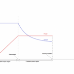
The Gate voltage should be 24 V as per the theoretical derivation,  but practically, the waveform observed has a peak to peak voltage of 22 V. This gives Vgs equal to 10 V (22 V -12 V) and that much voltage is sufficient enough to turn ON the MOSFET.

Graph showing Output Waveform of Half Bridge FET Circuit

Fig. 11: Graph showing Output waveform of half bridge FET circuit

The circuit designed in this tutorial can be used in designing of SMPS (switched mode power supply). It can be used in DC to AC converters and in induction heating applications. In the next tutorial, the modified sine wave inverter circuit will be completed by making full bridge MOSFET circuit and adding a step up transformer.


You may also like:


  • What are top applications of CAN protocol?

  • What are the different EV charging protocols?

  • What battery chemistries are used in electric vehicles?

  • What types of motors are used in electric vehicles?

  • What is the role of embedded software in electric vehicles?

  • What are the different types of electric vehicles?

Project Source Code

###


//Program to

/* code of bootstrap circuit for driving the high side MOSFET*/


// the setup function runs once when you press reset or power the board

void setup() {

  // initialize digital pin 2 and 3 as an output.

  pinMode(2, OUTPUT);   // at Hin pin of Ir2110 IC

    pinMode(3, OUTPUT);  // at Lin pin of Ir2110 IC

}


// the loop function runs over and over again forever

void loop() {


  //initially 2 and 3 pin are low 

  digitalWrite(3, HIGH);    //  Lin pin high

  delay(10);              // wait for 10ms second

  digitalWrite(3, LOW);     // Lin pin low

  delayMicroseconds(1);     // dead time of 1us

  digitalWrite(2, HIGH);     //  Hin pin high

 delay(10);              // wait for 10m second

 digitalWrite(2, LOW);     //  Hin pin LOW

 delayMicroseconds(1);     // dead time of 1us

  } 

###


Circuit Diagrams

Circuit-Diagram-Gate-Driver-Circuit-Modified-Sine-Wave-Inverter

Project Video


Filed Under: Power, Tutorials


Next Article

← Previous Article
Next Article →

Questions related to this article?
👉Ask and discuss on Electro-Tech-Online.com and EDAboard.com forums.


Tell Us What You Think!! Cancel reply

You must be logged in to post a comment.

EE TECH TOOLBOX

“ee
Tech Toolbox: Internet of Things
Explore practical strategies for minimizing attack surfaces, managing memory efficiently, and securing firmware. Download now to ensure your IoT implementations remain secure, efficient, and future-ready.

EE Learning Center

EE Learning Center
“engineers
EXPAND YOUR KNOWLEDGE AND STAY CONNECTED
Get the latest info on technologies, tools and strategies for EE professionals.

HAVE A QUESTION?

Have a technical question about an article or other engineering questions? Check out our engineering forums EDABoard.com and Electro-Tech-Online.com where you can get those questions asked and answered by your peers!


RSS EDABOARD.com Discussions

  • Reducing "shoot-through" in offline Full Bridge SMPS?
  • High Side current sensing
  • How to simulate power electronics converter in PSpice?
  • Voltage mode pushpull is a nonsense SMPS?
  • Layout IRN reduction in Comparator

RSS Electro-Tech-Online.com Discussions

  • Back to the old BASIC days
  • Parts required for a personal project
  • PIC KIT 3 not able to program dsPIC
  • Failure of polypropylene motor-run capacitors
  • Siemens large industrial PLC parts

Featured – RPi Python Programming (27 Part)

  • RPi Python Programming 21: The SIM900A AT commands
  • RPi Python Programming 22: Calls & SMS using a SIM900A GSM-GPRS modem
  • RPi Python Programming 23: Interfacing a NEO-6MV2 GPS module with Raspberry Pi
  • RPi Python Programming 24: I2C explained
  • RPi Python Programming 25 – Synchronous serial communication in Raspberry Pi using I2C protocol
  • RPi Python Programming 26 – Interfacing ADXL345 accelerometer sensor with Raspberry Pi

Recent Articles

  • What is AWS IoT Core and when should you use it?
  • AC-DC power supply extends voltage range to 800 V DC
  • Infineon’s inductive sensor integrates coil system driver, signal conditioning circuits and DSP
  • Arm Cortex-M23 MCU delivers 87.5 µA/MHz active mode
  • STMicroelectronics releases automotive amplifiers with in-play open-load detection

EE ENGINEERING TRAINING DAYS

engineering

Submit a Guest Post

submit a guest post
Engineers Garage
  • Analog IC TIps
  • Connector Tips
  • Battery Power Tips
  • DesignFast
  • EDABoard Forums
  • EE World Online
  • Electro-Tech-Online Forums
  • EV Engineering
  • Microcontroller Tips
  • Power Electronic Tips
  • Sensor Tips
  • Test and Measurement Tips
  • 5G Technology World
  • Subscribe to our newsletter
  • About Us
  • Contact Us
  • Advertise

Copyright © 2025 WTWH Media LLC. All Rights Reserved. The material on this site may not be reproduced, distributed, transmitted, cached or otherwise used, except with the prior written permission of WTWH Media
Privacy Policy

Search Engineers Garage

  • Electronic Projects & Tutorials
    • Electronic Projects
      • Arduino Projects
      • AVR
      • Raspberry pi
      • ESP8266
      • BeagleBone
      • 8051 Microcontroller
      • ARM
      • PIC Microcontroller
      • STM32
    • Tutorials
      • Audio Electronics
      • Battery Management
      • Brainwave
      • Electric Vehicles
      • EMI/EMC/RFI
      • Hardware Filters
      • IoT tutorials
      • Power Tutorials
      • Python
      • Sensors
      • USB
      • VHDL
    • Circuit Design
    • Project Videos
    • Components
  • Articles
    • Tech Articles
    • Insight
    • Invention Stories
    • How to
    • What Is
  • News
    • Electronic Product News
    • Business News
    • Company/Start-up News
    • DIY Reviews
    • Guest Post
  • Forums
    • EDABoard.com
    • Electro-Tech-Online
    • EG Forum Archive
  • DigiKey Store
    • Cables, Wires
    • Connectors, Interconnect
    • Discrete
    • Electromechanical
    • Embedded Computers
    • Enclosures, Hardware, Office
    • Integrated Circuits (ICs)
    • Isolators
    • LED/Optoelectronics
    • Passive
    • Power, Circuit Protection
    • Programmers
    • RF, Wireless
    • Semiconductors
    • Sensors, Transducers
    • Test Products
    • Tools
  • Learn
    • eBooks/Tech Tips
    • Design Guides
    • Learning Center
    • Tech Toolboxes
    • Webinars & Digital Events
  • Resources
    • Digital Issues
    • EE Training Days
    • LEAP Awards
    • Podcasts
    • Webinars / Digital Events
    • White Papers
    • Engineering Diversity & Inclusion
    • DesignFast
  • Guest Post Guidelines
  • Advertise
  • Subscribe