In tutorial 6 of this series, we built a circuit for D Morgan’s Theorems in Verilog, verifying its output to prove the theorems. (If you haven’t been following along, we highly recommend reviewing the previous tutorials before proceeding with this one. The first tutorial starts here.)
In this tutorial, we’ll:
- Write a Verilog program to build all other gates (AND, OR, NOT, XOR, NOR, etc.) using only the NAND gate.
- Verify the output waveform of the program (the digital circuit) with the truth tables of the AND, OR, NOT, XOR, and NOR gates.
Digital circuit

Truth table

Now, let’s write the Verilog program, compile and simulate it, and generate the output as a waveform. Then, we’ll verify the output waveforms against the given truth table.
(Please refer to the step-by-step procedure in Verilog Tutorial 3 to create a project, edit and compile the program, create a waveform file, simulate the program, and generate output waveforms.)
Verilog program
Gate-level modeling:
module nand_uni_gate(a,b,y_not,y_and,y_or,y_xor,y_xnor,y_nor);
input a, b;
output y_not,y_and,y_or,y_xor,y_xnor,y_nor;
wire t1,t2,t3,t4,t5,a_not,b_not;
nand(y_not,a,a);
nand(t1,a,b);
nand(y_and,t1,t1);
nand(a_not,a,a);
nand(b_not,b,b);
nand(y_or,a_not,b_not);
nand(t2,a_not,b_not);
nand(y_nor,t2,t2);
nand(t3,a_not,b);
nand(t4,a,b_not);
nand(y_xor,t3,t4);
nand(t5,t3,t4);
nand(y_xnor,t5,t5);
endmodule
Dataflow modeling:
module nand_uni_gate(a,b,y_not,y_and,y_or,y_xor,y_xnor,y_nor);
input a, b;
output y_not,y_and,y_or,y_xor,y_xnor,y_nor;
wire t1,t2,t3,t4,t5,t6,t7;
assign y_not = ~(a & a);
assign t1 = ~(a & b);
assign y_and = ~(t1 & t1);
assign t2 = ~ (a & a);
assign t3 = ~ (b & b);
assign y_or = ~(t2 & t3);
assign t4 = ~(~a & b);
assign t5 = ~(a & ~b);
assign y_xor = ~(t4 & t5);
assign t6 = ~(t4 & t5);
assign y_xnor = ~(t6 & t6);
assign t7 = ~(t2 & t3);
assign y_nor = ~(t7 & t7);
endmodule
(To learn more about Verilog programs, be sure to review Verilog tutorial 1 and Verilog tutorial 2 of these series.)
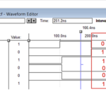
Now, compile the above program by creating a waveform file with all of the inputs and outputs listed. Then, simulate the project, and you should get the following result.
Simulation waveform

The output waveforms show that the gate circuits built using only NAND gates produce the same outputs as the respective standard gates. This demonstrates that all other gates can be constructed using only NAND gates, proving that the NAND gate is a universal gate.
In the next tutorial, we’ll prove that the NOR gate is also a universal gate by designing AND, OR, NOT, NAND, and XNOR gates using only the NOR gate.
You may also like:


Filed Under: Tutorials
Questions related to this article?
👉Ask and discuss on EDAboard.com and Electro-Tech-Online.com forums.
Tell Us What You Think!!
You must be logged in to post a comment.